- 您现在的位置:买卖IC网 > Sheet目录2098 > MK2069-04GILFTR (IDT, Integrated Device Technology Inc)IC VCXO CLK TRANSLATOR 56-TSSOP
DATASHEET
VCXO-BASED UNIVERSAL CLOCK TRANSLATOR
MK2069-04
IDT VCXO-BASED UNIVERSAL CLOCK TRANSLATOR
1
MK2069-04
REV J 051310
Description
The MK2069-04 is a VCXO (Voltage Controlled Crystal
Oscillator) based clock generator that features a PLL
(Phase-Locked Loop) input reference divider and feedback
divider that have a wide numeric range selectable by the
user. This enables a complex PLL multiplication ratio that
can be used for translation between clock frequency
standards.
The on-chip VCXO produces a stable, low jitter output clock
using a phase detector frequency down to 8 kHz or lower.
This means the MK2069-04 can translate between clock
frequencies that have a low common denominator, such as
the 8 kHz frame clock common with telecom standards. The
MK2069-04 also provides jitter attenuation of the input
clock and can accept a low input frequency as well.
The device is optimized for user configurability by providing
access to all major PLL divider functions. No power-up
programming is needed as configuration is pin selected.
External VCXO loop filter components provide an additional
level of user configurability.
The MK2069-04 includes a lock detector (LD) output that
serves as a clock status monitor. The clear (CLR) input
enables rapid synchronization to the phase of a newly
selected input clock.
Features
Input clock frequency <1 kHz to 170 MHz
Output clock frequency of 500 kHz to 160 MHz
Clock translation examples:
T1 (1.544 MHz) to/from E1 (2.048 MHz)
T3 (44.736 MHz) to/from E3 (34.368 MHz)
OC-3 (155.52 MHz) to/from T1 (1.544 MHz)
CCIR-601 (27 MHz) to/from SMPTE 274M (74.125
MHz)
Jitter attenuation of input clock provided by VCXO circuit.
Jitter transfer characteristics user configured through
external loop filter component selection.
Low jitter and phase noise generation.
PLL lock status output
PLL Clear function allows seamless synchronizing to an
altered input clock phase
2nd PLL provides frequency translation of VCXO PLL
output (VCLK) to a higher or alternate output frequency
(TCLK).
Device will free-run in the absence of an input clock
based on VCXO frequency.
56-pin TSSOP package
Single 3.3 V power supply
5 V tolerant clock input
Pb (lead) free package
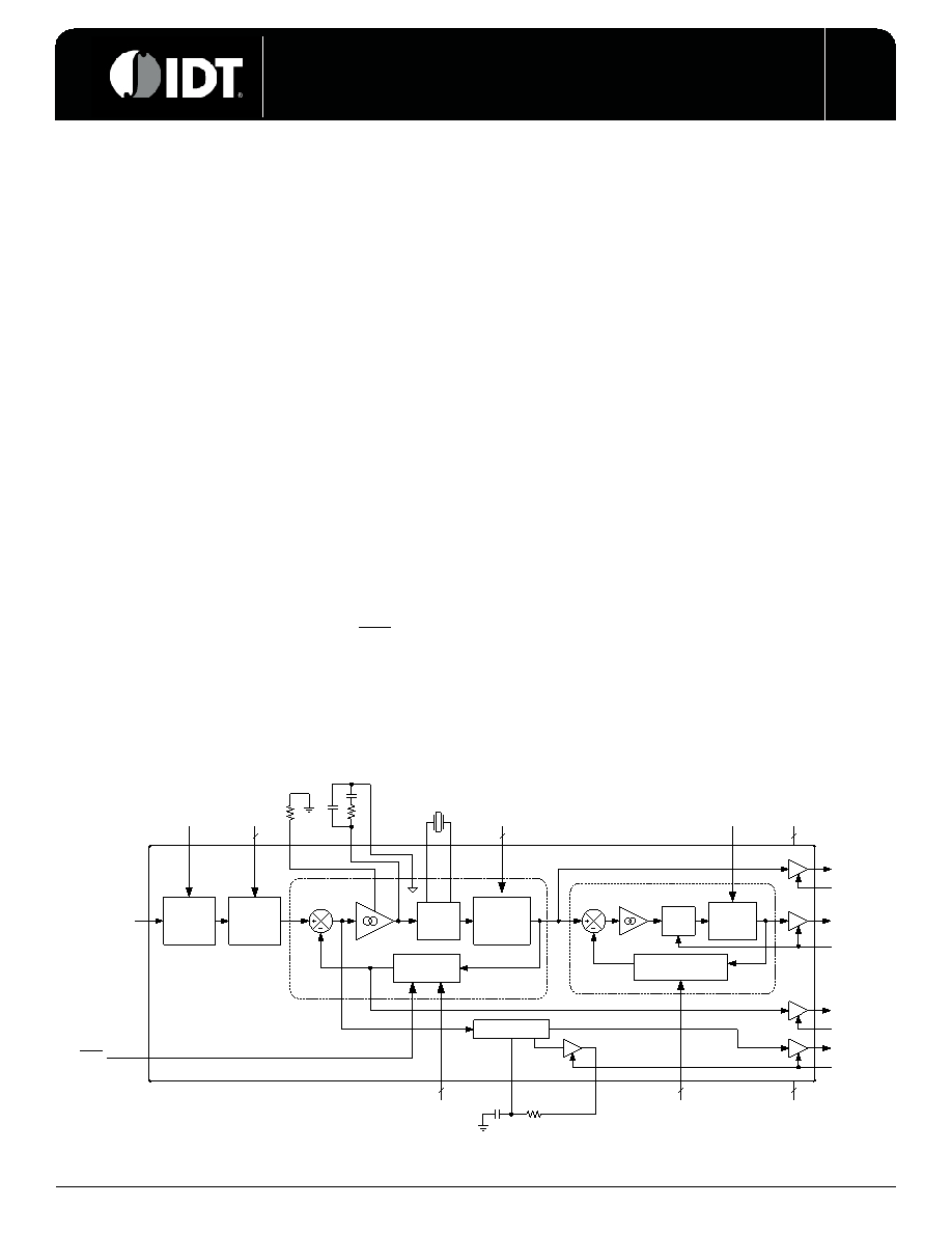
Block Diagram
C h arge
Pum p
VC XO
P u lla b le
xtal
VC LK
X2
X1
ISET
4
VD D
4
CL R
LF
FV D iv ide r
1 to 40 96
RV
Div id e r
2 to 40 97
SV
Div id e r
1,2,12 ,1 6
IC L K
RV 1 1 :0
12
P has e
Detecto r
VC XO
PLL
FT D iv id e r
2 to 16, ev en o n ly
ST
Div id e r
2, 16
VC O
T ra n slato r
PL L
SV1 :0
2
F V 11:0
FT 2 :0
3
ST
TC L K
OE V
OE T
LD
OE L
GN D
RCL K
OE R
Loc k D e te c tor
12
LD R
LF R
RP V
Div id e r
1, 8
RP V
LD C
发布紧急采购,3分钟左右您将得到回复。
相关PDF资料
MK2302S-01LFTR
IC MULTIPLIER/ZD BUFFER 8-SOIC
MK2304S-2LF
IC PLL ZD BUFFER LO SKEW 8-SOIC
MK2703SILF
IC PLL AUD CLK SYNTHESIZER 8SOIC
MK2704SLF
IC PLL AUD CLK SYNTHESIZER 8SOIC
MK2716SLFTR
IC CLK SYNTHESIZER HDTV 8-SOIC
MK2732-06GLF
IC VCXO/MULTIPLIER 16-TSSOP
MK2745-21SLFTR
IC CLK SOURCE DVD/MPEG 16-SOIC
MK2745-24SLF
IC CLK SOURCE DVD/MPEG 16-SOIC
相关代理商/技术参数
MK2069-04GITR
功能描述:IC VCXO CLK TRANSLATOR 56-TSSOP RoHS:否 类别:集成电路 (IC) >> 时钟/计时 - 时钟发生器,PLL,频率合成器 系列:- 标准包装:39 系列:- 类型:* PLL:带旁路 输入:时钟 输出:时钟 电路数:1 比率 - 输入:输出:1:10 差分 - 输入:输出:是/是 频率 - 最大:170MHz 除法器/乘法器:无/无 电源电压:2.375 V ~ 3.465 V 工作温度:0°C ~ 70°C 安装类型:* 封装/外壳:* 供应商设备封装:* 包装:*
MK206N 454634/1/MK
制造商:NSF (CONTROLS) 功能描述:WAFER MK 2POLE 6 POS 制造商:NSF (CONTROLS) 功能描述:WAFER, MK, 2POLE, 6 POS 制造商:NSF (CONTROLS) 功能描述:WAFER, MK, 2POLE, 6 POS; For Use With:Rotary Switches; No. of Poles:2; No. of Positions:6; SVHC:No SVHC (19-Dec-2012); Contact Current @ Contact Voltage AC Max:500mA; Contact Current AC Max:5A; Contact Current DC Max:5A; Contact ;RoHS Compliant: Yes
MK206S 454634MK
制造商:NSF (CONTROLS) 功能描述:WAFER MK 2POLE 6 POS 制造商:NSF (CONTROLS) 功能描述:WAFER, MK, 2POLE, 6 POS 制造商:NSF (CONTROLS) 功能描述:WAFER, MK, 2POLE, 6 POS; No. of Poles:2; No. of Positions:6; SVHC:No SVHC (19-Dec-2012); Contact Current @ Contact Voltage AC Max:500mA; Contact Current AC Max:5A; Contact Current DC Max:5A; Contact Current Rating:5A; Contact ;RoHS Compliant: Yes
MK20-B-100W
功能描述:近程传感器 1 Form A Cylindrical Term.
RoHS:否 制造商:Vishay Semiconductors 感应方式:Optical 感应距离:1 mm to 200 mm 电源电压:2.5 V to 3.6 V 安装风格:SMD/SMT 输出配置:Digital 最大工作温度:+ 85 C 最小工作温度:- 25 C 系列:VCNL3020
MK20-B-100W_DE
制造商:MEDER 制造商全称:Meder Electronic 功能描述:(deutsch) MK Reed Sensor
MK20-B-500W
制造商:MEDER 制造商全称:Meder Electronic 功能描述:MK Reed Sensor
MK20-B-500W_DE
制造商:MEDER 制造商全称:Meder Electronic 功能描述:(deutsch) MK Reed Sensor
MK20-C-100W
制造商:Willow Technologies 功能描述:MICRO REED SENSOR